
MOSIS 2.0
CA DREAMS is anchored by the new MOSIS 2.0, an extension of the well-known multi-project wafer (MPW) fabrication service launched by USC in 1981 that became self-sustaining by 1987. MOSIS provided affordable access to nascent silicon technologies for academia, industry, and government. Since its founding, MOSIS has supported 50+ US government laboratories and agencies, 800+ colleges and universities, and 100+ companies. MOSIS has trained thousands of microelectronic design engineers, launched the fabless semiconductor model, and been financially self-sustaining for over 35 years.
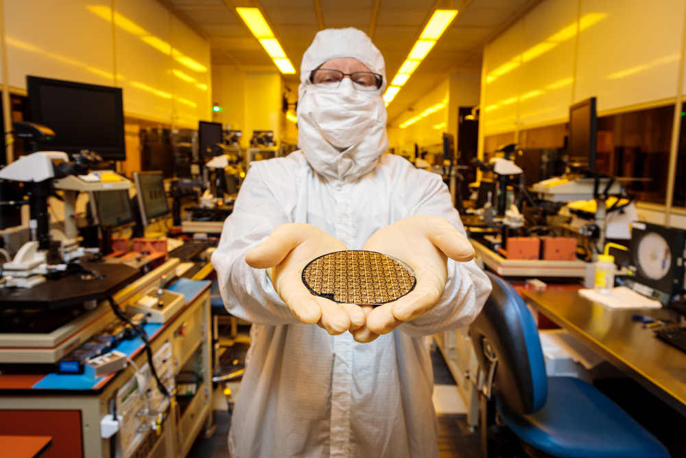
Now, MOSIS 2.0 builds upon the legacy of the original MOSIS service, aiming to accelerate prototyping in the state-of-the art analog compound semiconductor space. MOSIS 2.0 serves as a storefront and central gateway between customers and our end-to-end prototyping services, thereby reducing the barriers to innovation. The service features a secure data and analytic architecture to support electronic design automation (EDA) tools, a manufacturability analytics platform, and connectivity to government and CA DREAMS-curated intellectual property (IP).
Lab-to-Fab Facilities

The CA DREAMS hub integrates the operations of seven major research universities in Southern California with nanofab laboratories and three defense industrial base nanofabs that are capable of producing at the scale required by the Department of War. A key aspect of MOSIS 2.0 is its focus on scaling the advanced process and prototyping technologies within the hub toward eventual transition to high-volume production. This is accomplished by exploiting uniform process control and evaluation methods across the superhub. To achieve this, MOSIS 2.0 is pioneering the use of advanced data analytics techniques to optimize tool use and up-time and to inform the overall standardization process.
CA DREAMS provides accelerated prototyping and lab-to-fab transition capabilities for advanced integrated circuit (IC) development across a full range of technology platforms. Customer engagements are tailored to address a wide diversity of fabrication project types – ranging from short turnaround unit process prototyping to full flow IC prototyping to fullflow volume IC manufacturing. Projects are enabled by state-of-the-art nanofab and foundry services – covering compound semiconductors and Si within the hub – with pre-developed processes, pre-negotiated terms, a cloud-based integrated data and analytics architecture and a dedicated Prototype Integration and Engineering Service (PIES) team.
7 LABS, 3 FABS
University Nanofab Laboratories
- Caltech - Kavli Nanoscience Institute (KNI)
- UCI - Integrated Nanosystems Research
- UCLA - California NanoSystems Institute (CNSI)
- UC Riverside - UCR Nanofabrication Facility
- UCSB - UCSB Nanofabrication
- UCSD - San Diego Nanotechnology
- USC - John O’Brien Nanofab Laboratory
DoW-scale Fabs
PROCESS INTEGRATION AND ENGINEERING SERVICES (PIES) TEAM
The Process Integration and Engineering Services (PIES) team includes engineers from each university and industrial nanofab within the superhub, with expertise in the full range of deposition, etching, lithography, and metrology tools deployed in the superhub for a variety of technology platforms. Each project is shepherded through the nanofab facilities by a PIES engineer who has specific “hands-on” expertise in the nanofab tools and procedures needed for the project and is responsible for designing and executing the project within the superhub. The deployment of CA DREAMS’ superhub facilities is coordinated via the MOSIS 2.0 service, which coordinates the PIES team to provide the wide diversity of support needed across the spectrum of project types.
CA DREAMS RAPID PROTOTYPING FLOW
