
Latest News
MOSIS 2.0 and GlobalFoundries Partnership: A Strategic Alliance for Semiconductor Innovation
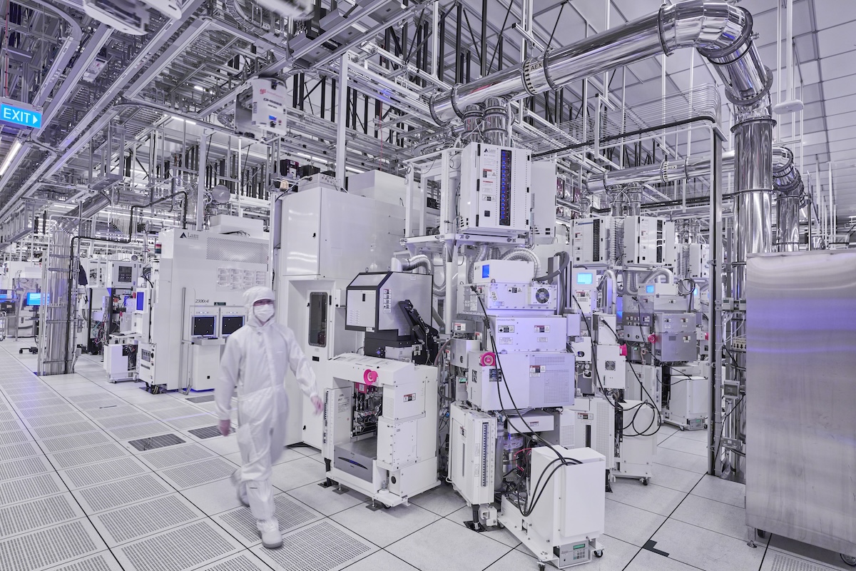
In a move that promises to broaden access to U.S.-based chip manufacturing, MOSIS 2.0 has signed a value-added partner agreement with GlobalFoundries (GF), one of the world's largest semiconductor manufacturers, creating a powerful synergy between the two industry partners.
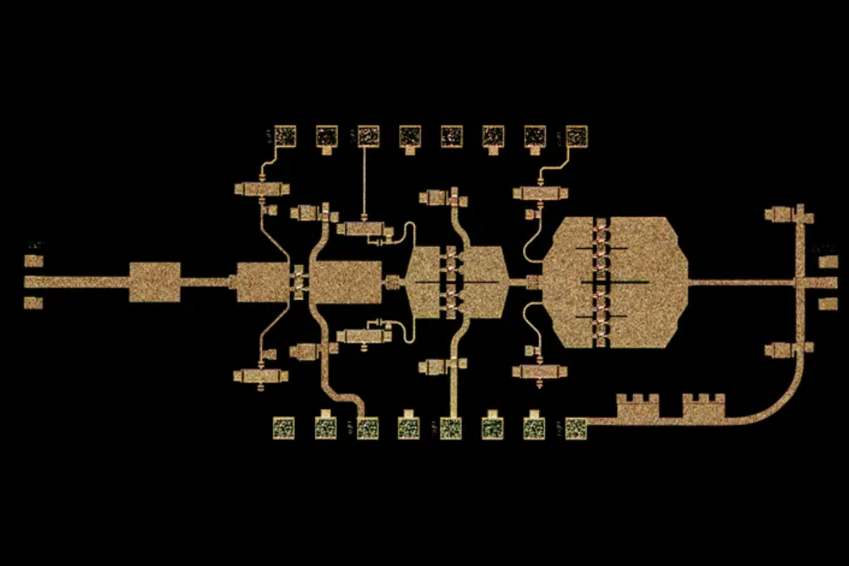
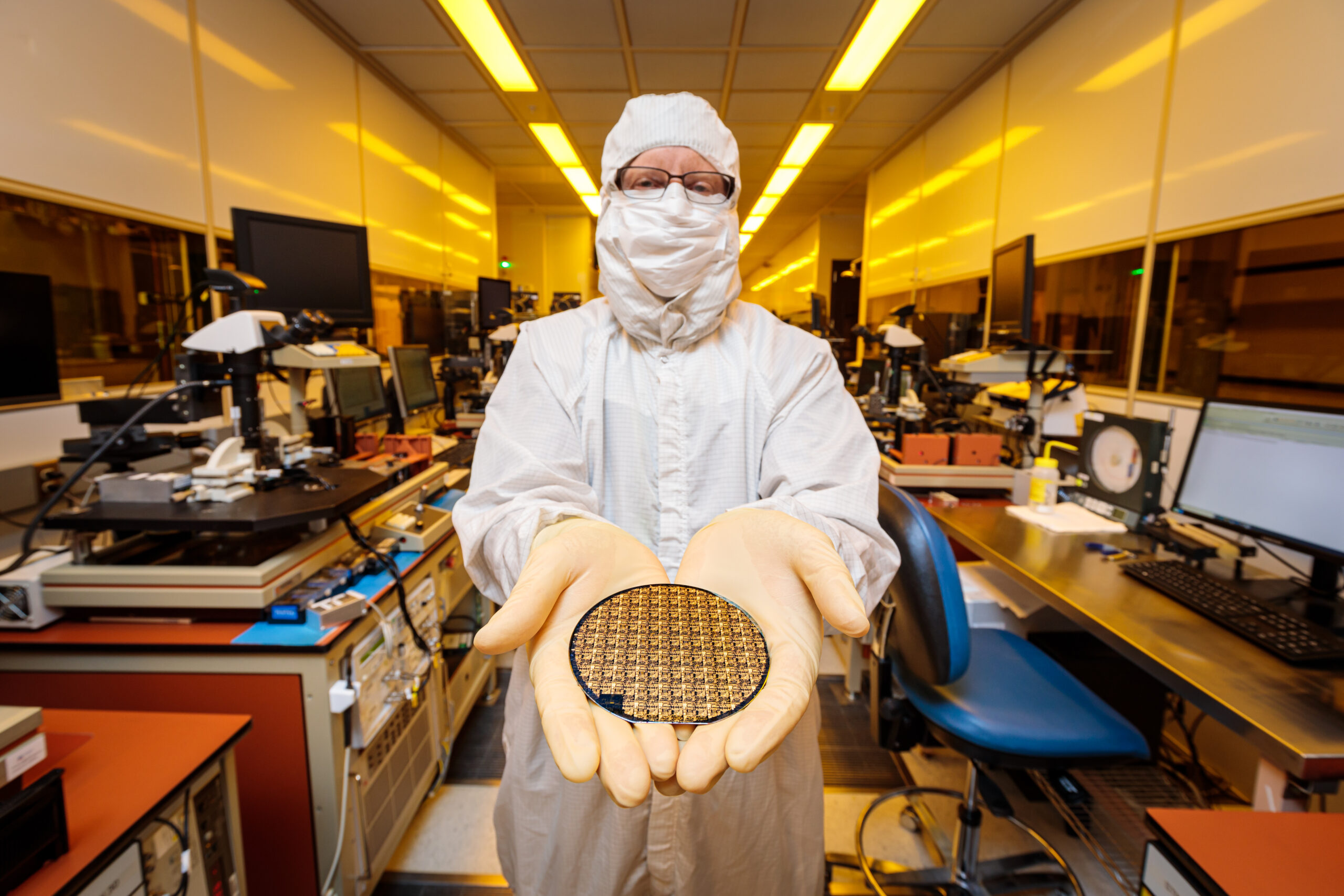
GaN Chip Developed Through CA DREAMS Delivers on Performance in Record Time
Northrop Grumman has developed a breakthrough GaN chip and brought it to market in under six months. The project was supported through California DREAMS and the DoW Microelectronics Commons.

CA DREAMS and Northrop Grumman Push Semiconductor Projects into High Gear
The latest phase of two major projects to advance chip technology aims to raise the bar to best-in-the-world performance.
Advanced Foundry Capabilities Through MOSIS 2.0
USC-led semiconductor prototyping initiative MOSIS 2.0 will be the official storefront for cutting-edge foundry services from domestic microelectronics leaders.
MOSIS 2.0: Powering the Next Generation of Breakthroughs Through Aggregation
MOSIS 2.0 Director Rehan Kapadia joined the latest episode of the Micro Journeys Podcast, where he discussed the intersection of imagination, engineering, and access in the world of microelectronics.
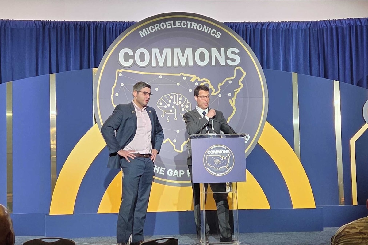
California DREAMS Showcases Semiconductor Impact on the National Stage
The USC-led semiconductor superhub highlighted its innovation and workforce development leadership at the 2026 Microelectronics Commons Annual Meeting in Washington, D.C.
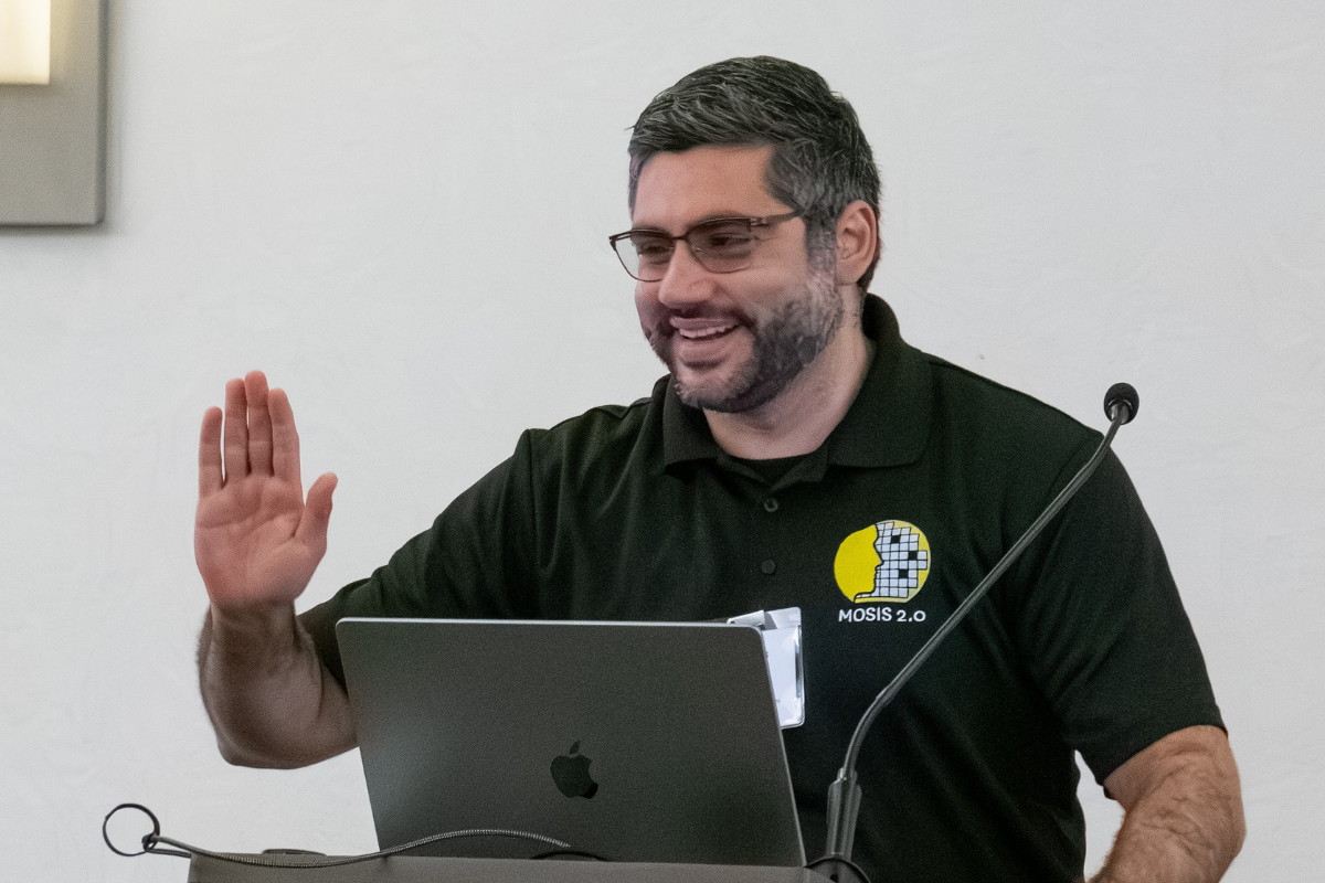
MOSIS 2.0 Revives a Legacy: Rehan Kapadia Outlines a Bold Future for Rapid Microelectronics Prototyping
Rehan Kapadia, director of MOSIS 2.0, shared how the service is building on its pioneering legacy to create a national network that lowers barriers, accelerates prototyping, and drives U.S. innovation in microelectronics.

California Semiconductor Workforce Data Reveals Major Gap Between Industry Projections and Reality
USC-led study challenges assumptions about technician demand as chip manufacturing expands, and demonstrates a shortage in engineers. This new job posting screening system could be used to monitor workforce needs in real time for any industry.
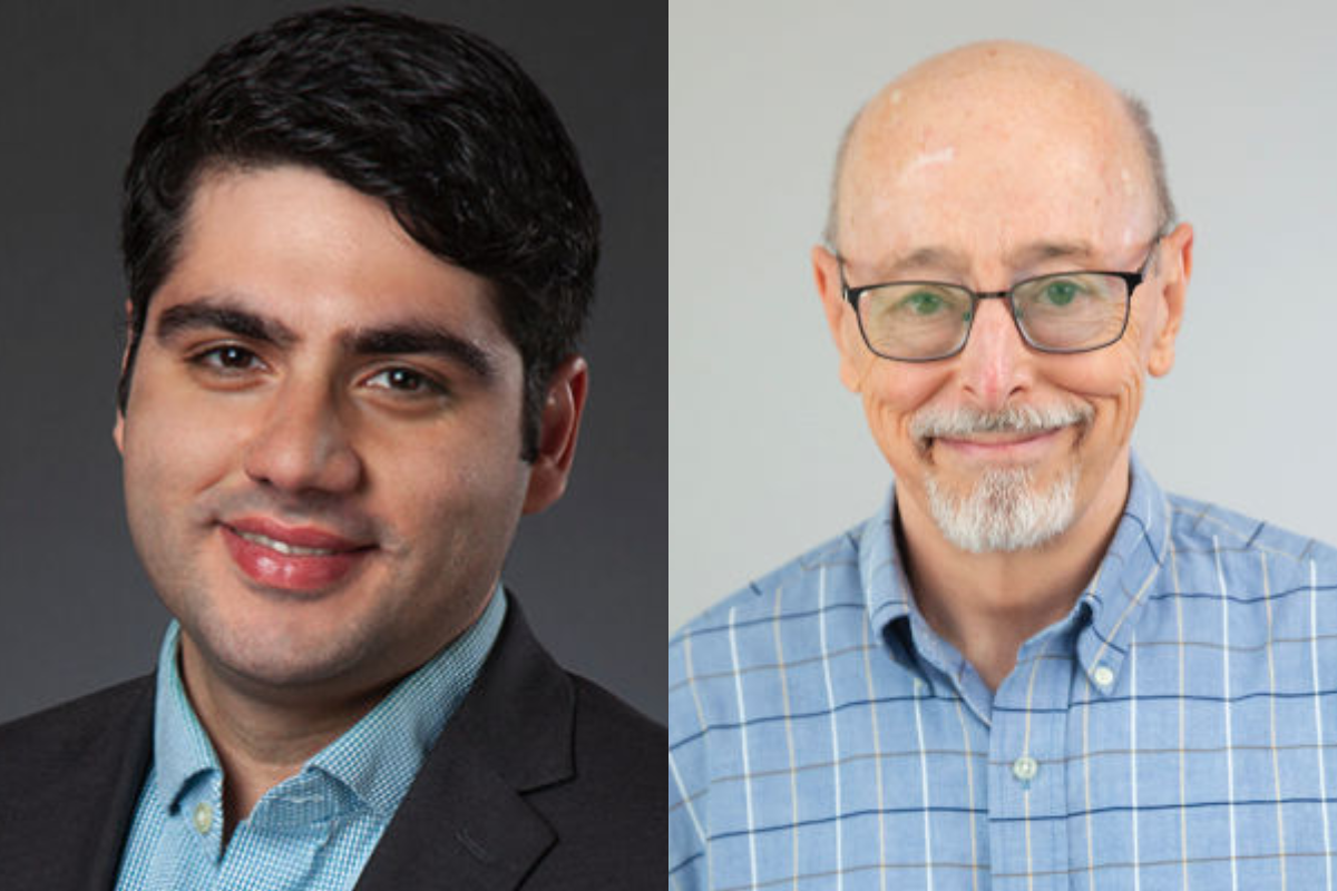
Rehan Kapadia Named Director of MOSIS 2.0
As CA DREAMS’ semiconductor fabrication service transitions to full-scale operations, Rehan Kapadia, a longtime faculty contributor and director of the USC John O’Brien Nanofabrication Laboratory, is named the new Director of MOSIS 2.0. Kapadia brings a strong vision for advancing MOSIS 2.0’s mission to accelerate semiconductor prototyping.
Integrating SWAP and MMEC Technologies into MOSIS 2.0
In 2025, MOSIS 2.0, is significantly expanding its semiconductor prototyping capabilities beyond Southern California to include technologies from two additional technology hubs: the Southwest Advanced Prototyping (SWAP) Hub, led by the Arizona Board of Regents on behalf of Arizona State University, and the Midwest Microelectronics Consortium (MMEC) Hub in Ohio.