
News
MOSIS 2.0 Revives a Legacy: Rehan Kapadia Outlines a Bold Future for Rapid Microelectronics Prototyping
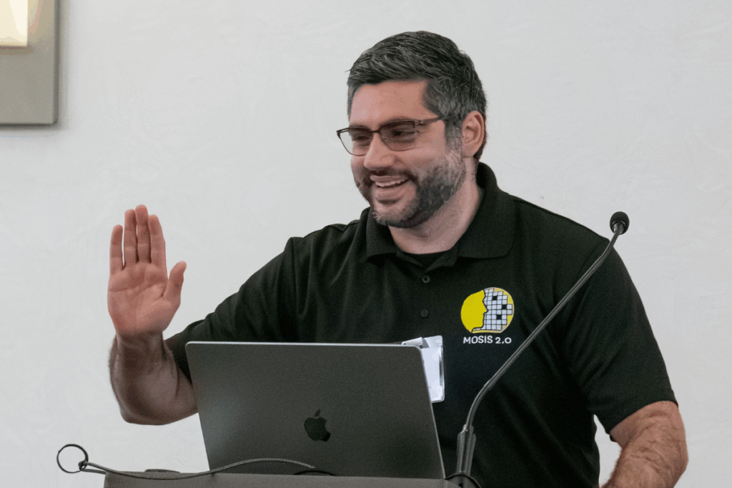
Rehan Kapadia, director of MOSIS 2.0, shared how the service is building on its pioneering legacy to create a national network that lowers barriers, accelerates prototyping, and drives U.S. innovation in microelectronics.
Read MoreCalifornia Semiconductor Workforce Data Reveals Major Gap Between Industry Projections and Reality
USC-led study challenges assumptions about technician demand as chip manufacturing expands, and demonstrates a shortage in engineers. This new job posting screening system could be used to monitor workforce needs in real time for any industry.
Read MoreRehan Kapadia Named Director of MOSIS 2.0
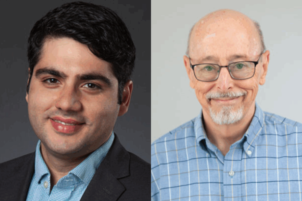
As CA DREAMS’ semiconductor fabrication service transitions to full-scale operations, Rehan Kapadia, a longtime faculty contributor and director of the USC John O’Brien Nanofabrication Laboratory, is named the new Director of MOSIS 2.0. Kapadia brings a strong vision for advancing MOSIS 2.0’s mission to accelerate semiconductor prototyping.
Read MoreIntegrating SWAP and MMEC Technologies into MOSIS 2.0
In 2025, MOSIS 2.0, is significantly expanding its semiconductor prototyping capabilities beyond Southern California to include technologies from two additional technology hubs: the Southwest Advanced Prototyping (SWAP) Hub, led by the Arizona Board of Regents on behalf of Arizona State University, and the Midwest Microelectronics Consortium (MMEC) Hub in Ohio.
Read MoreCA DREAMS welcomes AIT Taiwan Delegation
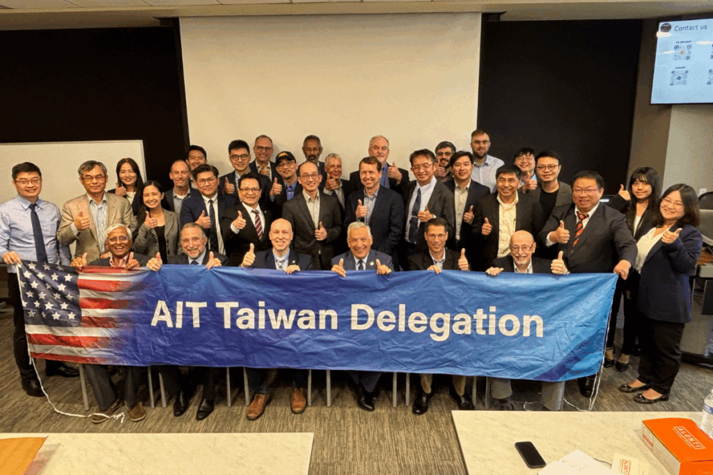
CA DREAMS hosted a distinguished delegation from the American Institute in Taiwan (AIT) at the University of Southern California. The visit marked a step toward deepening commercial and technological ties between the U.S. and Taiwan—particularly in the fields of semiconductors and microelectronics.
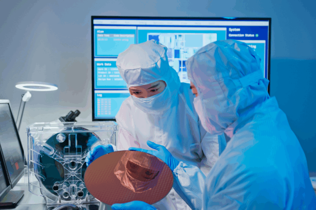
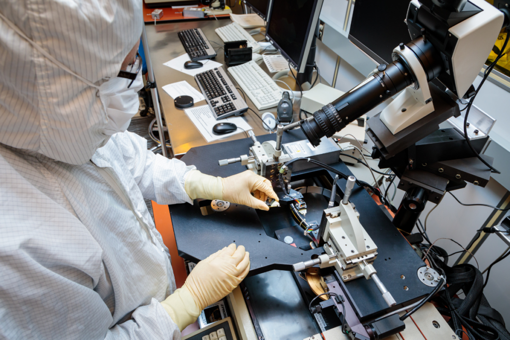
Read MoreMicroelectronics Go from Lab to Fab at UC San Diego’s Qualcomm Institute
UC San Diego’s work is part of the California DREAMS hub, a Southern California regional coalition of universities, contractors and workforce-development organizations led by the USC Viterbi School of Engineering and its Information Sciences Institute (ISI).
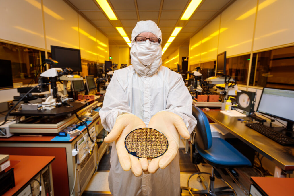
Read MoreMOSIS 2.0’s First Year: Bridging Research and Production
Over four decades, MOSIS delivered more than 60,000 integrated circuit designs and generated up to $10 million annually at its peak. Now, its successor, MOSIS 2.0, is advancing this legacy to address the next-generation of chip innovation.
Read MoreTwo projects accelerate CA DREAMS

For its second year of operation, hub partner Northrop Grumman leads two major projects: one aims to develop a next-generation semiconductor material known as gallium nitride (GaN), and the other aims to create advanced prototypes for faster, more reliable, next-generation wireless networks.
Read MoreIEEE Offers New Credential to Address Tech Skills Gap
Last year IEEE collaborated with the University of Southern California, in Los Angeles, and the California DREAMS on a microcredentialing program to give learners industry-relevant skills in semiconductor fabrication.
Read MoreUSC’s CA DREAMS Hub secures additional $27 million in DoD funding
The Department of Defense has awarded an additional $27 million from the CHIPS & Science Act to CA DREAMS. This continued investment will further support CA DREAMS in advancing U.S. semiconductor capabilities by expanding its infrastructure, operations, and workforce development.
Read More